Phys.org February 15, 2024
A team of researchers in the US (US Naval Research Laboratory, Kansas State University) demonstrated how hexagonal boron nitride (hBN) slabs tuned to the correct thickness act as optical waveguides, enabling direct optical coupling of light emission from encapsulated layers into waveguide modes. They integrated molybdenum selenide (MoSe2) and tungsten selenide (WSe2) within hBN-based waveguides and demonstrated direct coupling of photoluminescence emitted by in-plane and out-of-plane transition dipoles (bright and dark excitons) to slab waveguide modes. They demonstrated that dry etched hBN edges are an effective out-coupler of waveguided light without the need for oil-immersion optics. Gated photoluminescence of WSe2 demonstrated the ability of hBN waveguides to collect light emitted by out-of-plane dark excitons. Numerical simulations explored the parameters of dipole placement and slab thickness, and elucidatied the critical design parameters and serving as a guide for novel devices implementing hBN slab waveguides. The results provided a direct route for waveguide-based interrogation of layered materials, and a way to integrate layered materials into future photonic devices at arbitrary positions whilst maintaining their intrinsic properties… read more. TECHNICAL ARTICLE
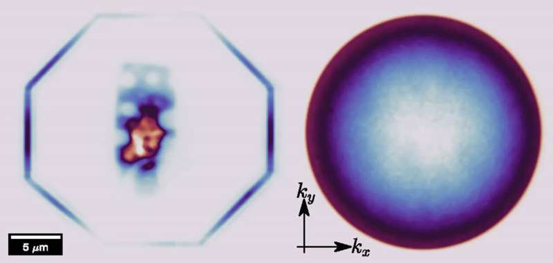
Real-space (left) and Fourier space (right) photoluminescence image of a hexagonal boron nitride waveguide…Credit: U.S. Naval Research Laboratory/Nicholas Proscia