Nanowerk July 26, 2023
The photosensitivity of silicon is inherently very low in the visible electromagnetic spectrum, and it drops rapidly beyond 800 nm in near-infrared wavelengths. Utilizing photon-trapping surface structures a team of researchers in the US (UC Davis, UC Santa Barbara, industry) demonstrated photoabsorption improvement in 1-μm-thin silicon, surpassing the inherent absorption efficiency of gallium arsenide for a broad spectrum. The photon-trapping structures allowed the bending of normally incident light by almost 90 deg to transform into laterally propagating modes along the silicon plane. The propagation length of light increased, contributing to more than one order of magnitude improvement in absorption efficiency in photodetectors, showed an enhanced photon density of states while substantially reducing the optical group velocity of light compared to silicon without photon-trapping structures, leading to significantly enhanced light–matter interactions. Simulations predicted an enhanced absorption efficiency of photodetectors designed using 30- and 100-nm silicon thin films that were compatible with CMOS electronics. According to the researchers despite a very thin absorption layer, such photon-trapping structures can enable high-efficiency and high-speed photodetectors with the potential for on-chip logic and optoelectronic integration… read more. Open Access TECHNICAL ARTICLE
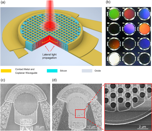
Schematic of the photon-trapping silicon MSM photodetector. Credit: Advanced Photonics Nexus, Vol. 2, Issue 5, 056001 (July 2023)