Phys.org February 23, 2023
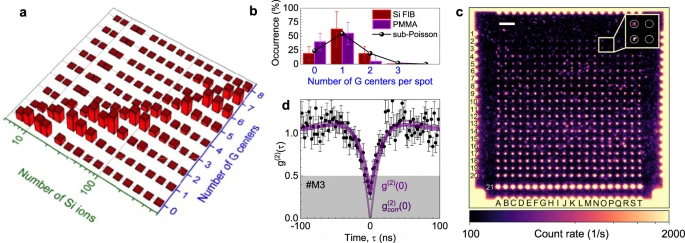
Monolithic integration of single-photon sources in a controllable way would give a resource-efficient route to implement millions of photonic qubits in photon integrated circuits. To run quantum computation protocols, these photons must be indistinguishable. Building on their previous work researchers in Germany have shown how focused ion beams from liquid metal alloy ion sources are used to place single-photon emitters at desired positions on the wafer while obtaining a high creation yield and high spectral quality. After several cooling-down and warming-up cycles, there was no degradation of their optical properties. To allow for wafer-scale engineering of individual photon emitters on the atomic scale compatible with established foundry manufacturing, the team implemented broad-beam implantation in a commercial implanter through a lithographically defined mask. They created dozens of telecom single-photon emitters at predefined locations with a spatial accuracy of about 50 nm. They emit in the strategically important telecommunication O-band and exhibited stable operation over days under continuous-wave excitation. According to the researchers the single-photon emitters are now technologically ready for production in semiconductor fabs and incorporation into the existing telecommunication infrastructure… read more. Open Access TECHNICAL ARTICLE
Wafer-scale nanofabrication of telecom single-photon emitters in silicon
Posted in Uncategorized and tagged Nanoscale fabrication, S&T Germany, Single photon emitters, Single-photon source.