MIT News January 18, 2023
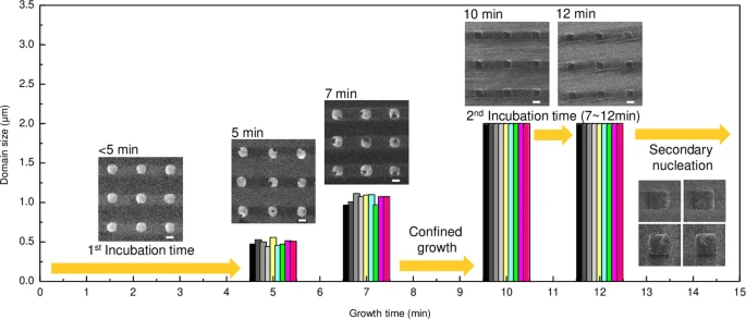
Two-dimensional materials and their heterostructures show a promising path for next-generation electronics. Nevertheless, 2D-based electronics have not been commercialized, owing mainly to three critical challenges: i) precise kinetic control of layer-by-layer 2D material growth, ii) maintaining a single domain during the growth, and iii) wafer-scale controllability of layer numbers and crystallinity. An international team of researchers (USA – MIT, UT Dallas, UC Riverside, Washington University, South Korea) has introduced a deterministic, confined-growth technique that can tackle these three issues simultaneously, thus obtaining wafer-scale single-domain 2D monolayer arrays and their heterostructures on arbitrary substrates. They geometrically confined the growth of the first set of nuclei by defining a selective growth area via patterning SiO2 masks on two-inch substrates. Owing to substantial reduction of the growth duration at the micrometre-scale SiO2 trenches, they obtained wafer-scale single-domain monolayer WSe2 arrays on the arbitrary substrates by filling the trenches via short growth of the first set of nuclei, before the second set of nuclei is introduced, thus without requiring epitaxial seeding. Further growth of transition metal dichalcogenides with the same principle yielded the formation of single-domain MoS2/WSe2 heterostructures. According to the researchers their work will lay a strong foundation for 2D materials to fit into industrial settings…read more. TECHNICAL ARTICLE
2 Lateral growth rate and secondary nucleation time for confined growth. Credit: Nature (2023)