Science Daily February 11, 2021
Graphene has been recently proposed to be integrated with silicon photonics to meet the challenges of next generation optical communication to increase the available bandwidth while reducing the size, cost, and power consumption of photonic integrated circuits. An international team of researchers (Italy, UK) focused on graphene photodetectors for high speed datacom and telecom applications based on the photo-thermo-electric effect, allowing for direct optical power to voltage conversion, zero dark current, and ultra-fast operation. They reported on a chemical vapour deposition graphene photodetector based on the photo-thermoelectric effect, integrated on a silicon waveguide, providing frequency response >65 GHz and optimized to be interfaced to a 50 Ω voltage amplifier for direct voltage amplification. They demonstrated a system test leading to direct detection of 105 Gbit s−1 non-return to zero and 120 Gbit s−1 4-level pulse amplitude modulation optical signals…read more. TECHNICAL ARTICLE 1 , Open Access 2
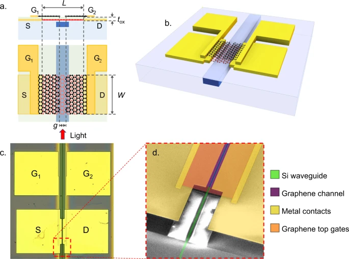
Structure of the realized device. Credit: Nature Communications volume 12, Article number: 806 (2021)