Phys.org July 3, 2023
Two-dimensional van der Waals materials are an excellent platform for the study of materials with well-defined interfaces. Signatures of acoustic phonons and defect states have been observed in current-to-voltage measurements. These features can be explained by direct electron–phonon or electron–defect interactions. An international team of researchers (Switzerland, Spain, Japan) used a tunnelling process that involved excitons in transition metal dichalcogenides (TMDs). They studied the tunnel junctions consisting of graphene and gold electrodes separated by hexagonal boron nitride with an adjacent TMD monolayer and observed prominent resonant features in current-to-voltage measurements appearing at bias voltages that corresponded to TMD exciton energies. By placing the TMD outside of the tunnelling pathway, they demonstrated that this tunnelling process does not require any charge injection into the TMD. According to the researchers the appearance of such optical modes in electrical transport introduces additional functionality towards van der Waals material–based optoelectronic devices… read more. Open Access TECHNICAL ARTICLE
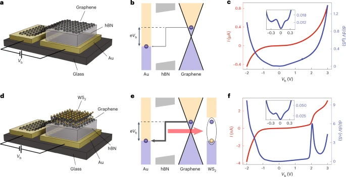
Device schematics, band diagrams and I−V characteristics. Credit: Nature Materials (2023)