MIT News April 27, 2023
Semiconductor chips are traditionally made with bulk materials, which are boxy 3D structures, so stacking multiple layers of transistors to create denser integrations is very difficult. Semiconductor transistors made from ultrathin 2D materials, each only about three atoms in thickness, could be stacked up to create more powerful chips. Using a low-temperature growth process that does not damage the chip, an international team of researchers (USA – MIT, Oak Ridge National Laboratory, Sweden) has demonstrated a novel technology that can effectively and efficiently “grow” layers of 2D transition metal dichalcogenide (TMD) materials directly on top of a fully fabricated silicon chip to enable denser integrations. They designed a metal–organic chemical vapour deposition reactor to separate the low-temperature growth region from the high-temperature chalcogenide-precursor-decomposition region. They obtained monolayer MoS2 with electrical uniformity on 200 mm wafers, as well as a high material quality with an electron mobility of ~35.9 cm2 V−1 s−1. They demonstrated a silicon-CMOS-compatible back-end-of-line fabrication process flow for MoS2 transistors; the performance of these silicon devices shows negligible degradation. According to the researchers this is an important step towards monolithic 3D integration for future electronics… read more. TECHNICAL ARTICLE
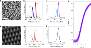
Material characterization. Credit: Nature Nanotechnology (2023)