Nanowerk November 9, 2022
Eliminating the etching process by directly fabricating nanowires onto the silicon substrate would lead to a marked improvement in the fabrication of spintronic devices. However, when directly fabricated nanowires are subjected to annealing, they tend to transform into droplets as a result of the internal stresses in the wire. Researchers in Japan have developed a new fabrication process to make L10-ordered CoPt nanowires on silicon/silicon dioxide (Si/SiO2) substrates. They coated a Si/SiO2 substrate with a material called a ‘resist’ and subjected it to electron beam lithography and evaporation to create a stencil for the nanowires, deposited a multilayer of CoPt on the substrate, ‘lifted-off’ the sample leaving behind CoPt nanowires. The nanowires were subjected to high temperature annealing. The nanowires took on L10-ordering induced by atomic interdiffusion, surface diffusion, and extremely large internal stress at the ultrasmall 10 nm scale curvature radii of the nanowires. The work may open a new field of research… read more. Open Access TECHNICAL ARTICLE
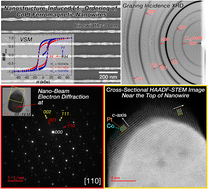
Graphical abstract. Credit: Nanoscale Adv., 2022, Advance Article