Science Daily August 16, 2022
The presence of piezoelectricity in 2D materials often depends on the number of layers. A team of researchers in the US (Rice University, UCLA, University of Houston, AF Laboratory Wright Patterson FB, Pennsylvania State University) made a one-dimensional, metal-semiconductor junction in a 2D heterostructure. A less than 10 nanometers thick junction was formed when tellurium gas was introduced while molybdenum metal formed a film on silicon dioxide in a chemical vapor deposition furnace. The process created islands of semiconducting molybdenum telluride phases in the sea of metallic phases. Applying voltage to the junction via the tip of a piezo response force microscope generated a mechanical response and measured the strength of piezoelectricity created at the junction. The discovery could aid in the development of ever-smaller nanoelectromechanical system to power tiny actuators and implantable biosensors, and ultrasensitive temperature or pressure sensors…read more. TECHNICAL ARTICLE
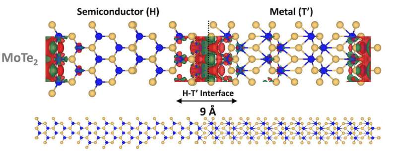
A charge redistribution model shows how charge flows across the phase interfaces in a 2D piezoelectric material of molybdenum (blue) and tellurium (yellow)…Credit: Advanced materials, 05 August 2022.