EurekAlert April 5, 2021
Wide-bandgap p-type oxides have carrier mobilities that are one to two orders of magnitude lower due to strong carrier localization near their valence band edge. Researchers in Australia have grown bilayer beta tellurium dioxide (β-TeO2) through the surface oxidation of a eutectic mixture of tellurium and selenium. It is theoretically proposed as a high-mobility p-type semiconductor. The isolated β-TeO2 nanosheets are transparent and have a direct bandgap of 3.7 eV. Field-effect transistors based on the nanosheets exhibit p-type switching with an on/off ratio exceeding 106 and a field-effect hole mobility of up to 232 cm2 V−1 s−1 at room temperature. A low effective mass of 0.51 was observed for holes, and the carrier mobility reached 6,000 cm2 V−1 s−1 on cooling to −50 °C. See-through devices could potentially be integrated in glass, in flexible displays, smart contact lenses and power electronics and communication technology…read more. TECHNICAL ARTICLE
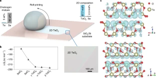
Schematic of tellurium oxide synthesis and transfer. Credit: Nature Electronics (2021)