Phys.org January 13, 2021
Low-dimensional materials can have a relatively small number of free charges and weak screening compared to 3-D materials. This screening is especially crucial for the development of tunnel field-effect transistors, which heavily rely on the quantum tunneling of electrons across junctions. By atomistic quantum transport simulations researchers in Canada show how bound charges can be engineered at interfaces of Si and low- oxides to strengthen screening. To avoid compromising gate control, low- and high- oxides are used in conjunction. They demonstrated that in Si nanowire tunnel field-effect transistors bound charge engineering increases the on-state current by orders of magnitude, and the combination of oxides yields minimal subthreshold swing. They concluded that the proposed bound-charge engineering paves a way toward improved low-power transistors…read more. TECHNICAL ARTICLE
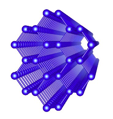
Image of one of the silicon nanowires that Prentki simulated in his work. Each sphere represents a silicon atom, and each bar represents an atomic bond between two neighboring silicon atoms. Credit: Prentki et al.