EurekAlert May 11, 2020
Using a room temperature grown locking layer and precise control over the entire fabrication process, a team of researchers in the US (NIST, University of Maryland) reduced unintentional dopant movement while achieving high quality epitaxy in scanning tunneling microscope (STM)-patterned devices. They demonstrated the exponential scaling of the tunneling resistance on the tunnel gap as it is varied from 7 dimer rows to 16 dimer rows, the capability to reproducibly pattern devices with atomic precision and a donor-based fabrication process where atomic scale changes in the patterned tunnel gap result in the expected changes in the tunneling rates. The research may lay the foundation for quantum computing…read more. Open Access TECHNICAL ARTICLE
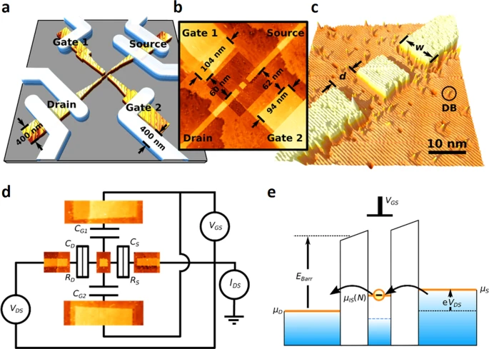
Scanning tunneling microscope (STM)-patterned single electron transistors (SETs). Credit: Communications Physics volume 3, Article number: 82 (2020)