Phys.org March 31, 2023
A Kondo lattice is often electrically insulating at low temperatures. However, several recent experiments have detected signatures of bulk metallicity within this Kondo insulating phase. An international team of researchers (USA – Harvard University, University of Illinois, University of Maryland, Stanford University, UK) visualized the real-space charge landscape within a Kondo lattice with atomic resolution using a scanning tunneling microscope. They discovered nanometer-scale puddles of metallic conduction electrons centered around uranium-site substitutions in the heavy-fermion compound uranium ruthenium silicide (URu2Si2) and around samarium-site defects in the topological Kondo insulator samarium hexaboride (SmB6). These defects disturbed the Kondo screening cloud, leaving behind a fingerprint of the metallic parent state. According to the researchers their results suggested that the three-dimensional quantum oscillations measured in SmB6 arise from Kondo-lattice defects, although they could not exclude other explanations. Their imaging technique could enable the development of atomic-scale charge sensors using heavy-fermion probes… read more. TECHNICAL ARTICLE
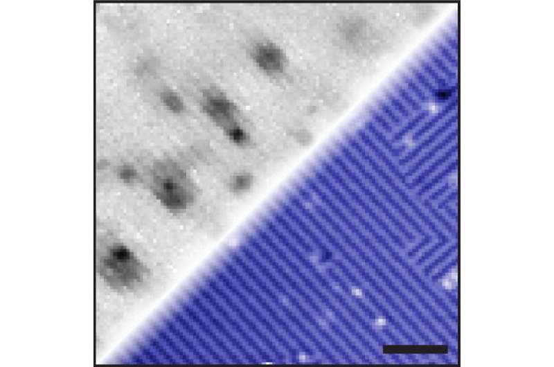
High-resolution image of an iron substitution… Credit: Harvard John A. Paulson School of Engineering and Applied Sciences.