Phys.org March 15, 2022
The high electron mobility of graphene points to great potential for broadband communications and high-speed electronics operating at terahertz switching rates. However, complex, and expensive fabrication methods make it more expensive and hinder mass production of such devices. Researchers in Sweden proposed chemical vapor deposition (CVD) of graphene on commercial copper (Cu) foils providing a scalable route towards high-quality single-layer graphene. The graphene is grown on a metallic surface like Cu, Pt or Ir, after which it can be separated from the metal and transferred to specifically required substrates. The process can be simply explained as carbon-bearing gasses that react at high temperatures (900–1100 degrees Celsius) in the presence of a metal catalyst, which serves both as a catalyst for the decomposition of the carbon species and as a surface for the nucleation of the graphene lattice. The researchers discovered that CVD graphene once transferred from copper to EVA/PET (ordinary lamination pouch) by hot press lamination, initially showed low carrier mobility in a range from 500—1000 cm2/(V s). But, once such films were kept at 60 C for several hours in a constant flow of nitrogen, the mobility increased eight times and reached 6000—8000 cm2/(V s) at room temperature… read more. Open Access TECHNICAL ARTICLE
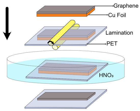
Process flow for graphene transfer from Cu foil to PET substrate. Credit: Nanomaterials 2022, Volume 12, Issue 3.