Nanowerk July 30, 2021
Incoming light can hit the electrons in the semiconductor lattice and move them to a higher energy state creating an electric field which further accelerates the high-energy electrons. They unload the extra energy by radiating it at different optical wavelengths, thus converting the wavelengths. An international team of researchers (USA – UCLA, Iowa State University, Germany) devised a solution for improving wavelength conversion using the semiconductor surface state phenomenon. They incorporated a nanoantenna array that bends incoming light, so it is confined around the shallow surface of the semiconductor converting the wavelength easily and without any extra added source of energy as the incoming light crosses the field. They converted a 1,550-nanometer wavelength light beam into the terahertz ranging from wavelengths of 100 micrometers up to 1 millimeter. For demonstration they incorporated the new technology into an endoscopy probe using terahertz waves. The technique can be applied to optical wavelength conversion in other parts of the electromagnetic spectrum, ranging from microwave to far-infrared wavelengths…read more. Open Access TECHNICAL ARTICLE
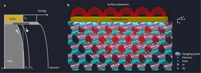
Energy band bending caused by the InAs surface states. Credit: Nature Communications volume 12, Article number: 4641 (2021)