Phys.org July 19, 2021
To create electrically conductive paths through a thick silicon dioxide researchers at UT Austin used a technique first deployed in the manufacturing of semiconductor electronic chips. By coating the silicon dioxide layer with a thin film of aluminum and heating the entire structure, arrays of nanoscale “spikes” of aluminum that completely bridge the silicon dioxide layer were created. These can be replaced by nickel or other materials that help catalyze the water-splitting reactions. When illuminated by sunlight, the devices efficiently oxidized water to form oxygen molecules while also generating hydrogen at a separate electrode and exhibited outstanding stability under extended operation. Because the techniques employed to create these devices are commonly used in manufacturing of semiconductor electronics, they should be easy to scale for mass production…read more. Open Access TECHNICAL ARTICLE
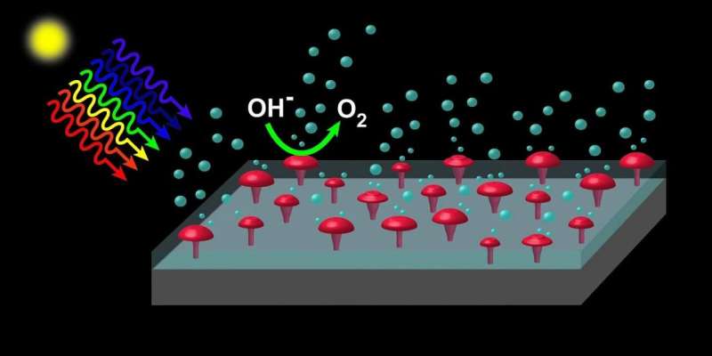
Graphic shows the basic geometry and functionality of the photoanode device. Credit: Cockrell School of Engineering, The University of Texas at Austin