Nanowerk June 10, 2021
Conventional infrared imaging technologies require the use of materials such as narrow bandgap semiconductors, which are sensitive to thermal noise and often require cryogenic cooling. An international team of researchers (Australia, Italy, UK, Germany, France, Bulgaria) developed and demonstrated a proof-of-concept compact all-optical device to perform infrared imaging in a metasurface composed of GaAs semiconductor nanoantennas using a nonlinear wave-mixing process. Experimentally they showed the upconversion of short-wave infrared wavelengths via the coherent parametric process of sum-frequency generation. In this process, an infrared image of a target is mixed inside the metasurface with a strong pump beam, translating the image from the infrared to the visible in a nanoscale ultrathin imaging device. The device is lightweight, cheap, and easy to mass produce, making them accessible to everyday users. The results open new opportunities for the development of compact infrared imaging devices with applications in infrared vision, life sciences and night-vision devices…read more. Open Access TECHNICAL ARTICLE
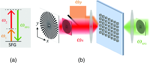
Energy level scheme of SFG mediated by a second-order nonlinear process… Credit: Advanced Photonics, 3(3), 036002 (2021).