Nanowerk February 16, 2021
Electro-absorption (EA) waveguide-coupled modulators are essential building blocks for on-chip optical communications. Compared to state-of-the-art silicon devices, graphene-based EA modulators promise smaller footprints, larger temperature stability, cost-effective integration, and high speeds. However, combining high speed and large modulation efficiencies in a single graphene-based device has remained elusive so far. An international team of researchers (Spain, Italy, Belgium) overcame this fundamental trade-off by demonstrating the 2D-3D dielectric integration in a high-quality encapsulated graphene device. They integrated hafnium oxide and two-dimensional hexagonal boron nitride within the insulating section of a double-layer graphene EA modulator. This combination of materials allows for a high-quality modulator device with high performances: a ~39 GHz bandwidth with a three-fold increase in modulation efficiency compared to previously reported high-speed modulators. The research paves the way to a plethora of electronic and opto-electronic devices with enhanced performance and stability, while expanding the freedom for new device designs…read more. Open Access TECHNICAL ARTICLE
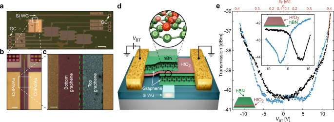
Device geometry and static characterization. Credit: Device geometry and static characterization. Nature Communications volume 12, Article number: 1070 (2021)