Nanowerk March 4, 2020
In conventional approaches of integrating III-V lasers on Si thick III-V buffers up to a few micrometers are used to reduce the defect densities, which posses huge challenges for efficient light interfacing between the epitaxial III-V lasers and the Si-based waveguides. Based on numerical simulations an international team of researchers (China, Hong Kong) designed and fabricated a novel growth scheme to eliminate the requirement of thick III-V buffers and thus promoted efficient light coupling into the Si-waveguides. They demonstrated the 1.5 µm III-V lasers directly grown on the industry-standard 220 nm SOI wafers using metal organic chemical vapor deposition. The lasers could sustain room-temperature and low-threshold lasing in 1.5 µm band under optical excitation. The research leads to the possibility and potential to monolithically integrate III-V lasers on the industry-standard 220 nm SOI wafers in an economical, compact and scalable way…read more. Open Access TECHNICAL ARTICLE
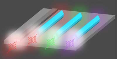
Schematic of III-V laser array directly grown on Si-photonics 220 nm SOI platform. (Image: HKUST)