Phys.org August 22, 2024
Two-dimensional materials (2DM) and their heterostructures offer tunable electrical and optical properties, primarily modifiable through electrostatic gating and twisting. Although electrostatic gating is a well-established method for manipulating Two-dimensional materials (2DM), achieving real-time control over interfacial properties remains challenging in exploring 2DM physics and advanced quantum device technology. Current methods are limited in their scope of application, lacking the accessibility and scalability of electrostatic gating at the device level. An international team of researchers (USA – Harvard University, MIT, Stanford University, UC Berkeley, Japan) introduced an on-chip platform for 2DM with in situ adjustable interfacial properties, using a MEMS comprising compact and cost-effective devices with the ability of precise voltage-controlled manipulation of 2DM, including twisting and pressurizing actions. They demonstrated the technology by creating synthetic topological singularities in the nonlinear optical susceptibility of twisted hexagonal boron nitride. A key application of this technology was the development of integrated light sources with real-time and wide-range tunable polarization. They predicted a quantum analogue that could generate entangled photon pairs with adjustable entanglement properties. According to the researchers their work extends the abilities of existing technologies and paves the way for new hybrid two- and three-dimensional devices, with promising implications in condensed-matter physics, quantum optics and related fields… read more. TECHNICAL ARTICLE
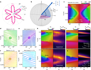
Experimental realization of synthetic merons (half-skyrmions) in the nonlinear susceptibility of twisted h-BN. Credit: Nature volume 632, pages1038–1044, 21 August 2024