Phys.org July 25, 2024
Current efforts to enable a broader range of optoelectronic functionality are limited because of inherent inefficiencies associated with spin injection across semiconductor interfaces. An international team of researchers (USA – National Renewable Energy Laboratory (NREL), University of Utah, Colorado School of Mines, University of Colorado, France) demonstrated spin injection across chiral halide perovskite/III–V interfaces achieving spin accumulation in a standard semiconductor III–V (AlxGa1−x)0.5In0.5P multiple quantum well light-emitting diode. The spin accumulation was detected through emission of circularly polarized light with a degree of polarization of up to 15 ± 4%. The chiral perovskite/III–V interface characterized with X-ray photoelectron spectroscopy showed a clean semiconductor/semiconductor interface at which the Fermi level could equilibrate. According to the researchers their findings demonstrated chiral perovskite semiconductors could transform well-developed semiconductor platforms into ones that can also control spin… read more. TECHNICAL ARTICLE
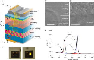
LED schematic and interface characterization. Credit: Nature volume 631, pages307–312, 19 June 2024