Phys.org July 3, 2024
When the tilting angles are arbitrary, the grain boundaries in atomically thin van der Waals materials form inhomogeneous sublattices, giving rise to local electronic states that are not controlled. An international team of researchers (Korea, USA – Harvard University) has reported on epitaxial realizations of deterministic MoS2 mirror twin boundaries (MTBs) at which two adjoining crystals are reflection mirroring by an exactly 60° rotation by position-controlled epitaxy. They showed that these epitaxial MTBs were one-dimensionally metallic to a circuit length scale. They incorporated the epitaxial MTBs as a 1D gate to build integrated two-dimensional field-effect transistors (FETs). In both individual and array FETs, they demonstrated state-of-the-art performances for low-power logics. According to the researchers their work suggests a novel synthetic pathway for the integration of two-dimensional FETs—that are immune to high gate capacitance—towards ultimate scaling… read more. TECHNICAL ARTICLE
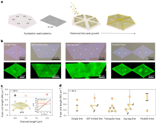
Designed 1D epitaxial metal network geometries by position-controlled nucleation. Credit: Nature Nanotechnology 3 July, 2024