Phys.org May 30, 2024
Previous investigations for thickness-scalable high dielectric constant (k) gate layers have failed to solve the “polarizability–scalability–insulation robustness issues. An international team of researchers (UK, China) showed that this problem could be solved by using a gate layer of a high k ferroelectric oxide in its superparaelectric (SPE) state. They showed that in the SPE, the polar order became local and was dispersed in an amorphous matrix with a crystalline size down to a few nanometers, leading to an excellent dimensional scalability and a good field-stability of the k value. As an example, a stable high k value was shown in ultrathin SPE films of (Ba0.95,Sr0.05)(Zr0.2,Ti0.8)O3 deposited on LaNiO3-buffered Pt/Ti/SiO2/(100)Si down to a 4 nm thickness, leading to a small equivalent oxide thickness of ~0.46 nm. The SPE film had high breakdown strength ensuring a low leakage current for the operation of the CMOS gate. The SPE films displayed a high electrical fatigue resistance. According to the researchers their results show the potential of superparaelectric materials as gate dielectrics in the next-generation microelectronics… read more. Open Access TECHNICAL ARTICLE
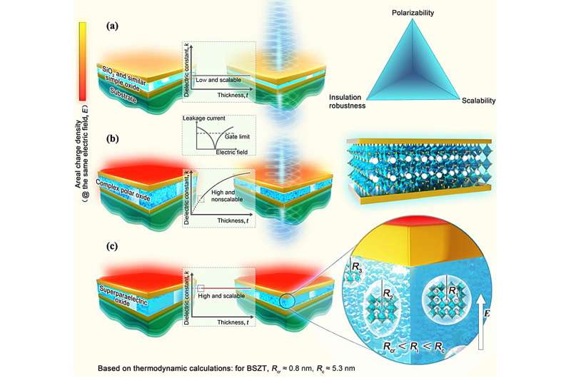
Using a superparaelectric high k dielectric to solve the trilemma in a gate layer… Credit: Journal of Advanced Ceramics, 2024, 13(4): 539-547